Laughing Hyena
  • Home
  • Hyena Games
  • Esports
  • NFT Gaming
  • Crypto Trends
  • Game Reviews
  • Game Updates
  • GameFi Guides
  • Shop
Tag:

TSMC

ASML
Product Reviews

TSMC reiterates it doesn’t need High-NA EUV for 1.4nm-class process technology

by admin May 29, 2025


TSMC reiterated its long-known stance on next-generation High-NA EUV lithography tools at its European Technology Symposium in Amsterdam. The company does not require these highest-end lithography systems for its next-generation process technologies, including A16 (1.6nm-class) and A14 (1.4nm-class) process technologies. To that end, TSMC will not adopt High-NA EUV tools for these nodes. 

“ People seems to always interested when TSMC going to use High-NA, I think our answer is very simple,” said Kevin Zhang, Deputy Co-COO and Senior Vice President of Business Development and Global Sales, at the event. “Whenever we see High-NA will provide meaningful, measurable benefit, we will do it. With A14, the enhancement I talked about earlier is very substantial without using High-NA. So, our technology team continues to find a way to extend the life of current EUV while harvesting the scaling benefit.”

TSMC’s A14 process relies on the company’s second-generation nanosheet gate-all-around transistors, along with a new standard cell architecture. According to TSMC, A14 provides up to 15% higher performance at the same power and complexity, or alternatively, 25% to 30% lower power consumption at the same frequency. In terms of transistor density, A14 achieves a 20% increase compared to N2 for mixed logic/SRAM/analog configurations and up to 23% when it comes to pure logic.


You may like

Such performance, power, and transistor density increases represent the so-called ‘full node advantage’, and yet, TSMC does not need next-generation High-NA EUV lithography tools to produce chips with predictable yields and desired performance and power characteristics on its A16 and A14 process technologies. One should keep in mind that TSMC’s A16 is essentially N2P with a Super Power Rail (SPR) backside power delivery network. As TSMC does not need High-NA EUV tools for N2 and N2P, it will not need them for A16 either. By contrast, A14 is an all-new node that will be used for mass production in 2028, so the fact that TSMC does not need High-NA for this one is quite remarkable.

When asked whether A14 heavily relies on multi-patterning, Zhang responded that he could not comment on specifics, but said that TSMC’s technology team had found a way to produce chips on a 1.4nm node without using High-NA EUV tools that provide an 8nm resolution compared to a 13.5nm resolution of Low-NA EUV systems.

“This is a great innovation from our technology team,” said Zhang. “As long as they continue to find a way, obviously, we do not have to use High-NA EUV. Eventually, we will use it at some point. It is just so we need to find a right interception point, provide the maximum benefit, maximum return on investment.”

It is noteworthy that TSMC’s A14 will be succeeded by A14 with SPR backside power delivery in 2029, and it does not appear that the foundry will require High-NA EUV tools for this iteration either. To that end, it looks like, unlike Intel, which is set to start using next-generation EUV lithography machines with its 14A manufacturing technology to reduce the number of EUV exposures (read: multipatterning) and process steps in 2027 – 2028, TSMC has no plans to use High-NA EUV for mass production until at least 2030, or perhaps even later.

Get Tom’s Hardware’s best news and in-depth reviews, straight to your inbox.

Follow Tom’s Hardware on Google News to get our up-to-date news, analysis, and reviews in your feeds. Make sure to click the Follow button.


Source link

May 29, 2025 0 comments
0 FacebookTwitterPinterestEmail
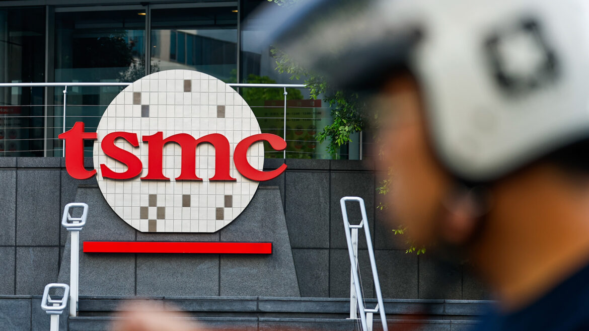
TSMC Lobby
Gaming Gear

TSMC to open up chip design center in Munich to help local chip developers

by admin May 28, 2025


TSMC is set to open its first chip design center in Munich, Germany, in a bid to help local and European chip developers optimize their designs to its process technology, the company announced at its European Technology Symposium in Amsterdam, the Netherlands.

The facility in Munich will perform multiple functions to simplify the implementation of chips on its process technologies, as well as helping partners on system-level design. Essentially, the center’s competencies will span from basic assistance in the development of tiny microcontroller units (MCUs) made using mature process technologies for the automotive industry to design technology optimization (DTCO) of advanced processors for AI and HPC applications that rely on leading-edge production nodes.

“We want to bring the best support to the European customer,” said Kevin Zhang, Deputy Co-COO and Senior Vice President of Business Development and Global Sales, at the event. “Here we want to have the design team to be able to directly work with the customer under our fab here, so we can bridge the product design and the manufacturing together. Lots of time we use the term DTCO — design technology co-optimization — [so that is what we are going to do in Munich].


You may like

The development center in Munich will be the company’s 10th facility of this kind, but the first one in Europe, which highlights the revival of European chip development in particular and the semiconductor industry in general. TSMC already has nine chip design centers across the world that are located in Canada, China, Japan, Taiwan, and the U.S.

In addition, the world’s largest contract maker of chips has Design Center Alliance (DCA) — a global network of companies — that provide chip implementation services as well as system-level design solutions. Ultimately, these companies can even design chips to order, something that TSMC’s own design centers are not meant to do.

TSMC — along with its partners Bosch, Infineon, and NXP — is currently building its first fab in Europe. The fab, which will be capable of building chips on TSMC’s N12 and N16 (12nm and 16nm-class), is mainly aimed at MCUs, but will certainly make other types of chips. To perform and yield optimally, all chips nowadays require design optimizations that may go beyond what EDA software offers, which is why TSMC needs its design center in Europe.

“It is not like you bring the technology there and you can do manufacturing for the rest of your life,” said Zhang. “That does not work that way. You need to work closely with your end customer to continue to make an improvement. So, by having a design team right here in the heart of the semiconductor land in Europe, we can bridge the customer and the technology manufacturing closer.”

Get Tom’s Hardware’s best news and in-depth reviews, straight to your inbox.

Follow Tom’s Hardware on Google News to get our up-to-date news, analysis, and reviews in your feeds. Make sure to click the Follow button.


Source link

May 28, 2025 0 comments
0 FacebookTwitterPinterestEmail

Categories

  • Crypto Trends (244)
  • Esports (185)
  • Game Reviews (177)
  • Game Updates (214)
  • GameFi Guides (245)
  • Gaming Gear (243)
  • NFT Gaming (232)
  • Product Reviews (249)
  • Uncategorized (1)

Recent Posts

  • If you want to play Elden Ring Nightreign in a duo, the Seamless Co-op mod is already out, dead simple to use, and it won’t mess up your vanilla save
  • Altcoin Season Odds Grow Strong As Alts Break Free From Bitcoin’s Shadow
  • Details emerge about canceled Black Panther game and the Nemesis System
  • Yooka-Laylee developer Playtonic is laying off over a dozen staff
  • 6 Great Games To End May With

Recent Posts

  • If you want to play Elden Ring Nightreign in a duo, the Seamless Co-op mod is already out, dead simple to use, and it won’t mess up your vanilla save

    May 31, 2025
  • Altcoin Season Odds Grow Strong As Alts Break Free From Bitcoin’s Shadow

    May 31, 2025
  • Details emerge about canceled Black Panther game and the Nemesis System

    May 31, 2025
  • Yooka-Laylee developer Playtonic is laying off over a dozen staff

    May 31, 2025
  • 6 Great Games To End May With

    May 31, 2025

Newsletter

Subscribe my Newsletter for new blog posts, tips & new photos. Let's stay updated!

About me

Welcome to Laughinghyena.io, your ultimate destination for the latest in blockchain gaming and gaming products. We’re passionate about the future of gaming, where decentralized technology empowers players to own, trade, and thrive in virtual worlds.

Recent Posts

  • If you want to play Elden Ring Nightreign in a duo, the Seamless Co-op mod is already out, dead simple to use, and it won’t mess up your vanilla save

    May 31, 2025
  • Altcoin Season Odds Grow Strong As Alts Break Free From Bitcoin’s Shadow

    May 31, 2025

Newsletter

Subscribe my Newsletter for new blog posts, tips & new photos. Let's stay updated!

@2025 laughinghyena- All Right Reserved. Designed and Developed by Pro


Back To Top
Laughing Hyena
  • Home
  • Hyena Games
  • Esports
  • NFT Gaming
  • Crypto Trends
  • Game Reviews
  • Game Updates
  • GameFi Guides
  • Shop

Shopping Cart

Close

No products in the cart.

Close